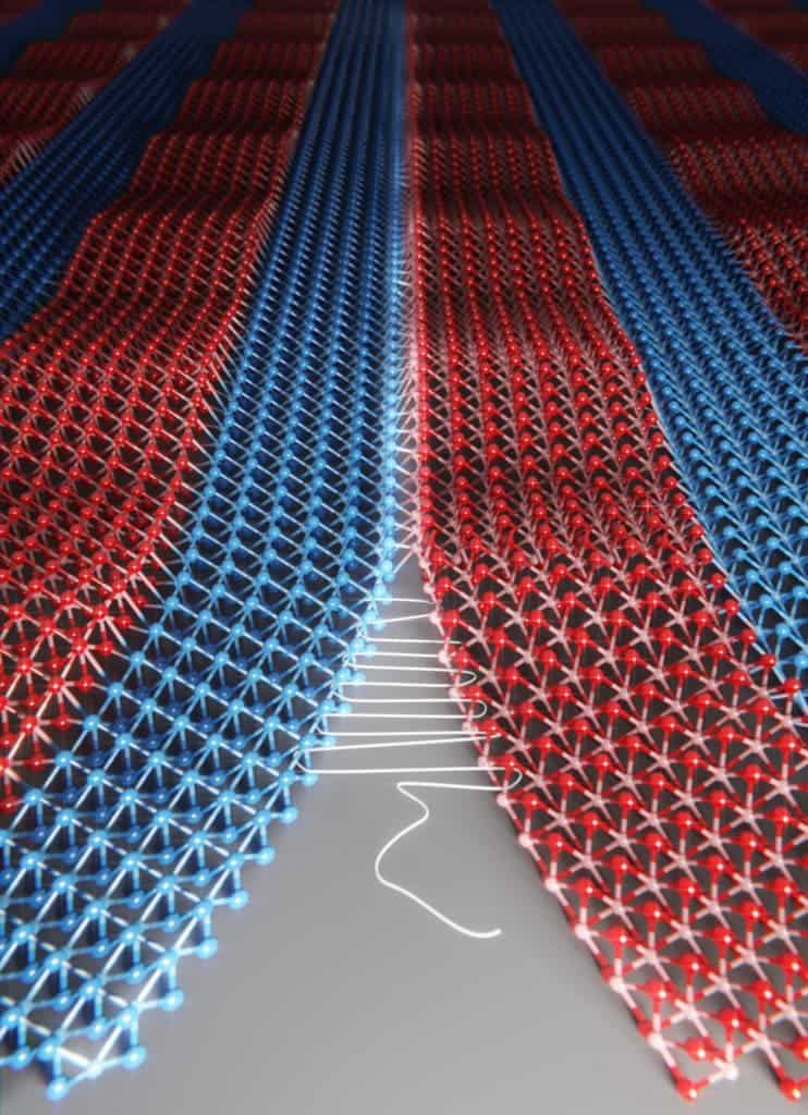
Researchers from the United States devised a clever new technique that basically “sews” two patches of different crystals seamlessly together. The interface between the two crystal is so smooth, it’s atom-thin. The findings could lead to a better performing electronics.
“Current electronics technology is based on bulk and thick materials and their heterostructures, we took a completely different approach to generate heterostructures—seamless stitching various thin crystals while maintaining the three-atom thickness throughout. These seamless, atomic fabrics not only exhibit similar functions with the conventional heterostructures but also show unique properties and promise for applications that are not available before,” Saien Xie, a graduate student at the University of Chicago and first author on the paper, told ZME Science.
Joining two or more different materials together can lead to highly desirable electrical properties. These arrangements are called heterojunctions, and have proven themselves as indispensable components in many modern electronics, from solar panels to computer chips. Often, the performance of such materials is predicated on how smooth the interface is between the junctions. The smoother the seam between two materials, the easier electrons flow across it.
Most often, the materials used in heterostructures are composed of crystals whose atoms are arranged in rigid lattices and which may have different spacing. When you combine different crystals, their configuration is never perfect.
In a new study, researchers at the University of Chicago and Cornell stitched together two patches of crystals to create atom-thick junctions. They devised a new technique that grew three-atom-thick crystals in a single session and in a constant environment. Typically, crystals are grown in stages and under very different conditions. “You grow one material first, stop the growth, change the condition, and start it again to grow another material,” said Jiwoong Park, professor of chemistry and lead author of the new study published in Science.
The resulting single-layer materials are the most perfectly aligned ever grown, say the researchers. Since the transition between the two sewn-together fabric-like lattices is so gentle, there are no holes or other defects at the interface.
“The main challenge was to find the optimum condition under which various atomic crystals can be synthesized with the same high quality. One Aha moment is that when we observed uniform ripples when we looked at the nanometer-scale height profile of the stitched atomic crystals. That was never seen before and was the signature of the seamless stitching of two atomic crystals. At that moment we realized that we had generated truly unique materials,” Xie said.
The performance was tested on a diode. When the two different kinds of material are joined, electronics are able to flow one way through the “fabric”, but not the other. Indeed, the three-atom-thick LEDs started glowing.
LEDs are currently manufactured by stacking them in 3D layers, rather than 2D, and usually on a rigid surface. The new technique devised by the researchers could lead to new kinds of flexible LEDs or atom-thick 2D circuits that can operate both horizontally and laterally. What’s more, stretching and compressing the ‘fabric’ resulted in changes in the optical properties of the crystals due to quantum mechanical effects — a quirk that could prove useful in light sensors and LEDs that change color as they stretch. The method is uniform multi-inch wafer scale; therefore, it could be scaled for production “after a modest amount of work,” according to Xie.
Next, the researchers plant to “explore the unique properties and applications of these “seamless atomic fabrics”, for example, color-tunable, high-efficiency LEDs and strain sensors,” Xie told me.
Scientific reference: “Coherent, atomically-thin transition-metal dichalcogenide superlattices with engineered strain.” Xie et. al, Science, March 8, 2018.


