Since the invention of the Atomic Force Microscope (AFM) in 1986, science has become increasingly reliant on these imaging instruments that allow spatial and time resolution like nothing that came before. Thousands of scientific papers are published each year in which AFMs are used to characterize materials, drugs, and more. Thanks to AFM, researchers are now closing in on the tiny particles that characterize misfolding diseases like Alzheimer’s, Parkinson’s, and Huntington’s disease, as well asdiabetes and tuberculosis. Nobel prizes have been won on the back of these instruments.
It would take a whole book to praise the achievements and progress enabled by these microscopes. But there’s always room for better, smarter, faster; and one company called Integrated Circuit Scanning Probe Microscopes (ICSPI Corp) says it can make an AFM that’s small, easy to use, and costs about 10x less than many high-end AFMs.
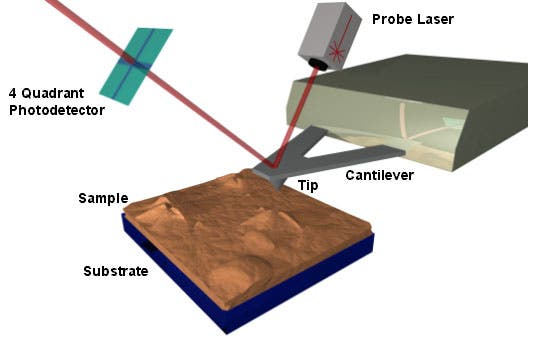
AFM works by bringing an atomically sharp tip close to a surface. There is an attractive force between the tip and the surface and this force is kept the same throughout the experiment. As the probe tip scans back and forth over the surface, the tip will rise and fall with the different features on the surface. Since all this is going on at a very small scale, we can’t watch the tip directly. A laser is pointed at the tip and the beam is reflected toward a sensor. As the tip goes up and down the laser hits different parts of the sensor. With the information the sensor collects, an image of the surface can be recreated.
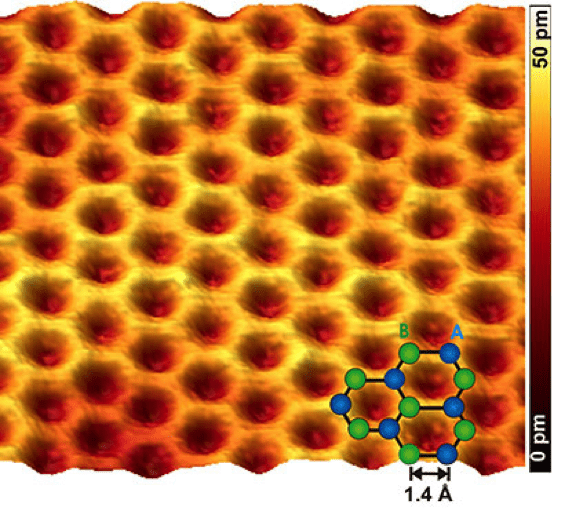
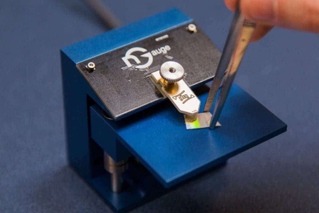
This drastic scale down, which has been in the works for the last decade, was made possible thanks to a 1x1mm silicon chip called the nGauge AFM chip. On this tiny chip, the researchers were able to stack a 3-axis MEMS scanner, a sharp tip, and a sensor to measure tip-sample interactions — all in a mind-bogglingly small volume.
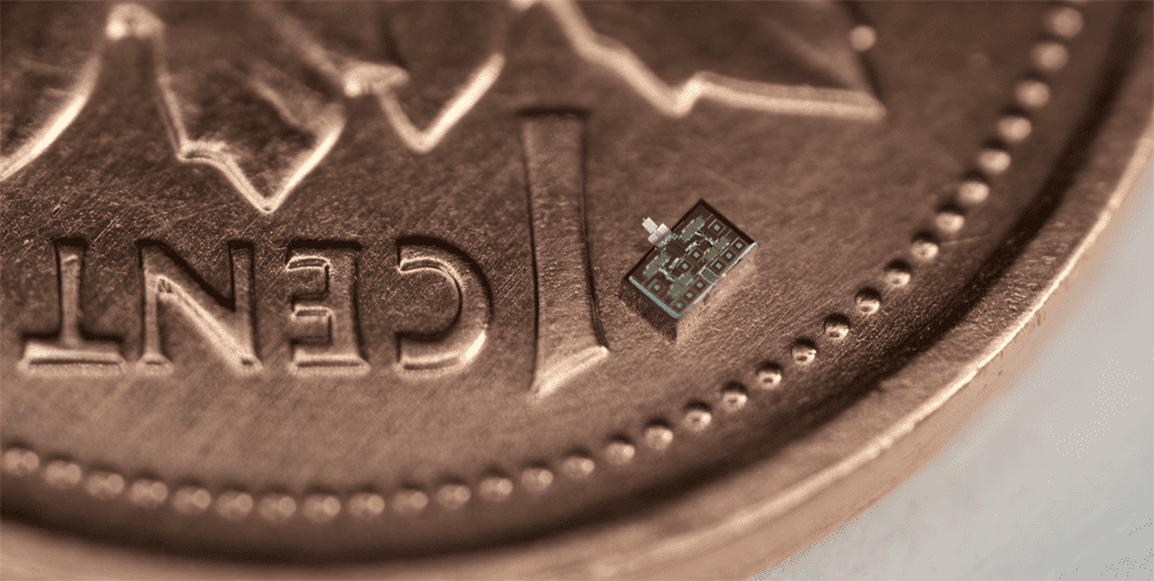
is a research-grade instrument that’s shrunk down by a factor of a million to fit onto a microchip. Credit: nGauge
“We succeeded in integrating all of the scanners, sensors, and the tip (essentially the entire AFM) onto a single 1x1mm chip. This eliminates the need for the bulky and expensive piezoelectric scanner stages and laser sensing systems used in conventional AFMs. The AFM chips are fabricated using CMOS technology, the same advanced technology that gives us processors, RAM, and virtually all microelectronics these days. CMOS manufacturing is vastly scalable and allows batch fabrication which drives down costs. An additional processing step is performed on the CMOS chips to “release” the micro-scale mechanical structures. These microstructures, called MEMS, are known to have extremely high resolution and sensitivity, making them perfectly suited for Atomic Force Microscopy,” Duncan Strathearn, one of the nGauge co-founders, told ZME Science.
A traditional AFM machine is very bulky, being around the size of a desk, and costs $100,000 onwards. ICSPI Corp, which is a Univesity of Waterloo spinoff, heavily innovated and managed to create a microscope that costs much less, with little compromise in quality compared to high-end AFMs. Moreover, the technology works better in some applications which require the imaging of nanoscale objects smaller than the wavelengths of light.

“While single-chip AFMs cannot currently achieve the sub-angstrom resolutions of today’s best AFMs,their performance is on par with mid-range systems. In fact they are actually superior to traditional AFMs in many ways. Their small size leads to improved vibration immunity, lower drift, and higher scan speeds. The compact form-factor can lead to new applications by easily enabling integration into standard equipment like probe stations, electron microscopes, or assembly lines. For the first time it’s also possible to place the AFM on the sample instead of the other way around. The complete integration also makes it straightforward to operate as there are no laser to align, and the tips are easy to exchange since the whole AFM chip is disposable. The fact that the chip is disposable means that it’s simple to stay up to date with the latest advances, as improved AFM chip designs will be released periodically,” Strathearn said.
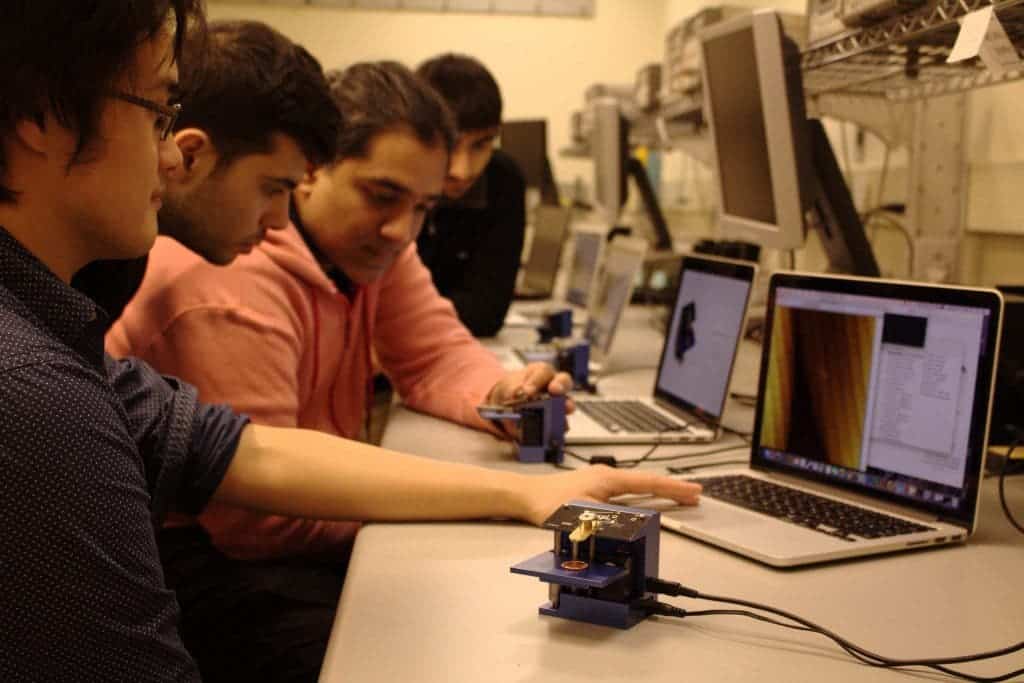
Strathearn and colleagues recently brought their nGauge microscope to a high school class, with great results. Most of these kids had never heard about an AFM, let alone use one. With such a substantial reduction in price, AFM imaging could be democratized and become widely available across classrooms — just as traditional optical telescopes are ubiquitous today. Looking at a magnified onion cell in a biology class can be a transformative experience, but imagine using an AFM to image DNA — all in high school. Then, there are countless university classrooms or startups whose work might now be brought to the next level thanks to this innovation.
“AFMs are very versatile instruments used for a variety of applications in research and industry. Up until now, the cost and complexity of these instruments have made them inaccessible to many potential users. The nGauge AFM’s unprecedented low cost and ease of use will enable access to nanoscale imaging for applications including fundamental research into cancer, quality control of electroplated or polished surfaces, and in-situ measurements in assembly lines, to name just a few. This technology will have a transformative impact on nanoscale science and metrology by opening up the fields to a wide range of new users while enhancing the capabilities of experienced AFM users,” Strathearn added.
More information on the nGauge is available on their website.

