Virtually all electronics today are based on silicon, with the semiconductor powering everything from microwave ovens to the world’s fastest supercomputers. Silicon is the most abundant element in the Earth’s crust, which makes it cheap and readily available, and is additionally very easy to manufacture into chips and wafers thanks to its crystalline structure. But although silicon has served us well, it’s far from perfect and starting to reach its limits.
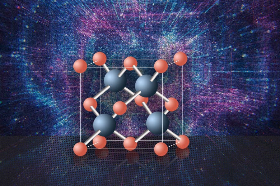
Researchers at MIT and the University of Houston have experimented with a new material called cubic boron arsenide, showing that the novel semiconductor can overcome a number of limitations that plague silicon and drag down some of its applications in electronics.
Much better than silicon, but can it pass the test of time?
While silicon crystals are great for conducting electrons, it far less accommodating for their “holes”, the second type of charge carrier that is responsible for generating an electric current in a semiconductor material. A hole can be seen as the “opposite” of an electron, although confusingly enough, holes aren’t really particles in the same way electrons are, rather they represent the absence of an electron in an atom.
Besides poor hole transfer, silicon also isn’t a good heat conductor, which explains why your smartphone will start to overheat a while after you use resource-intensive apps.
In order to overcome these limitations, scientists across the world have been experimenting with all sorts of alternatives, in search of the ‘golden grail’ of semiconductors. In 2018, researchers led by MIT professor of mechanical engineering Gang Chen theoretically predicted that cubic boron arsenide (c-BAs) should have an ultrahigh thermal conductivity comparable to diamond, as well as excellent electron-hole mobility. This combination of properties makes the material rather unique and an ideal building block for transistors.
Now, researchers employed special optical detection methods to probe the material experimentally at the smallest quantum level, confirming theoretical predictions made earlier.
According to the results reported in Science, boron arsenide has a stupendously high thermal conductivity that’s almost 10 times greater than that of silicon, while maintaining a comparable bandgap. The band gap is a non-permitted energy band between the valence band and the conduction band, so an electron in the valence band requires an amount of energy at least equal to the band gap in order to become a free electron. Having a band gap is what makes a material a semiconductor. Additionally, the researchers found cubic boron arsenide has high mobility for both electrons and holes.
“That’s important because of course in semiconductors we have both positive and negative charges equivalently. So, if you build a device, you want to have a material where both electrons and holes travel with less resistance,” Chen said in a statement.
Previously, researchers were only able to find semiconductors that have good mobility in one way, but poor mobility in the other. But boron arsenide is great for both electron and hole mobility — and this could make it a game changer in the industry.
Companies like Tesla have for some time stopped using silicon for their power electronics, replacing it with silicon carbide, which has around three times the thermal conductivity of silicon. Silicon carbide has poorer electron mobility than pure silicon though, but Tesla nevertheless still considers the material superior to silicon because it more than makes up for its shortcoming with enhanced performance due to better heat dissipation. Now, imagine what cubic boron arsenide could do with ten times the heat transfer and even better electron-hole mobility.
Chen likens this constellation of useful properties to those of graphene, often nicknamed the ‘wonder material’ because of its unique combination of exceptional properties. Graphene is not only the thinnest but also one of the strongest materials; it conducts heat better than all other materials; it is an excellent conductor of electricity; it is optically transparent, yet so dense that it is impermeable to gases – not even helium, the smallest gas atom, can pass through it.
“This is impressive, because I actually don’t know of any other material, other than graphene, that has all these properties,” he says. “And this is a bulk material that has these properties.”
These experiments were performed in the lab on a small scale. The challenge now lies in manufacturing cubic boron arsenide in sufficient quantities cheaply and usefully. At the moment, the main manufacturing method for this promising new semiconductor produces a nonuniform material that is not suitable for working applications in electronics. For comparison, the silicon used in today’s computer chips is about 99.99999999% pure. The researchers will also have to test how the material performs in time, as long-term stability can be another limiting factor in the way of large-scale adoption. So silicon will likely remain the king of semiconductors for some time, but its crown is definitely shacking.
“Silicon is the workhorse of the entire industry,” says Chen. “So, OK, we’ve got a material that’s better, but is it actually going to offset the industry? We don’t know.”


