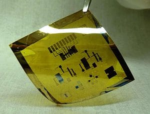
Nanocrystals have always interested researchers since their electrical and thermodynamic properties show strong size dependence, which could potentially lead to some highly efficient new technologies. Scientists at University of Pennsylvania recently showed that nanocrystals of semiconductor cadmium selenide can be easily printed or layered on-top of flexible plastics to form electronic devices. This could potentially open up a slew of new technological possibilities.

Your typical electronic circuit, which you can find inside just about any household electronics from remote controls to tablets, is layered on-top of a rigid board, 99% of the time a silicon wafer. By devising flexible electronics, a new range of applications might be opened, from smart clothing, to more agile robots. Finding the right technological mix between material availability and manufacturing cost is serious impediment, however.
“We have a performance benchmark in amorphous silicon, which is the material that runs the display in your laptop, among other devices,” said professor Cherie Kagan.
“Here, we show that these cadmium selenide nanocrystal devices can move electrons 22 times faster than in amorphous silicon.”
That’s fast, and not only that, they’re also easier to store and use. morphous silicon uses a process that operates at several hundred degrees; cadmium selenide nanocrystals can be deposited at room temperature and annealed at mild temperature. How did the researchers reach such incredible performances, though?
Well, the scientists took extra care when building their nanocrystals in order to ensure maximum compatibility with the binding flexible plastic surface. For one thing, the researchers employed special ligands – chemical chains that extend from the nanocrystals’ surfaces and helps facilitate conductivity as they are packed together into a film.
“There have been a lot of electron transport studies on cadmium selenide, but until recently we haven’t been able to get good performance out of them,” Kim said. “The new aspect of our research was that we used ligands that we can translate very easily onto the flexible plastic; other ligands are so caustic that the plastic actually melts.”
Since the nanocrystals are typically produced as an ink-like liquid, they can be easily stored through various methods, and most importantly they can be applied to surfaces extremely easily. For instance, the researchers used a simple stencil to etch small channels of conducting gold, which make the make the electrical connections to upper levels that would form the circuit. On top of this, an insulating aluminum oxide layer was introduced and again on top of this a 30-nanometer layer of nanocrystals was coated. Finally, in the last step electrodes on the top level were deposited through shadow masks. Using this technique, the researchers built three devices: an inverter, an amplifier and a ring oscillator.
“The more complex circuits are like buildings with multiple floors,” Kagan said. “The gold acts like staircases that the electrons can use to travel between those floors.”
“An inverter is the fundamental building block for more complex circuits,” Lai said. “We can also show amplifiers, which amplify the signal amplitude in analog circuits, and ring oscillators, where ‘on’ and ‘off’ signals are properly propagating over multiple stages in digital circuits.”
“And all of these circuits operate with a couple of volts,” Kagan said. “If you want electronics for portable devices that are going to work with batteries, they have to operate at low voltage or they won’t be useful.”
Findings were detailed in the journal Nature Communications.
via Kurzweil AI


