Among its many stellar properties, graphene is an amazing electrical conductor. However, if graphene is to reach its full potential in the field of electronics, it needs to coaxed to turn current on or off like silicon transistors. Physicists at the Department of Energy’s Oak Ridge National Laboratory (ONRL) present a recent breakthrough that may enable graphene to act like a semiconductor. The catch is to grow graphene in curled nanoribbons rather than in flat 2-D sheets.

When arranged in wide sheets, the hexagon-linked graphene doesn’t have a band gap, which means you can’t use it in modern electronics like computer chips or solar panels. It’s a great electrical wire but useless as a transistor. That’s speaking about its traditional configuration because graphene can work as a semiconductor in other arrangements. Doping graphene with various impurities can enable the material to switch on or off, for instance, DNA and copper ions as demonstrated previously by another team.
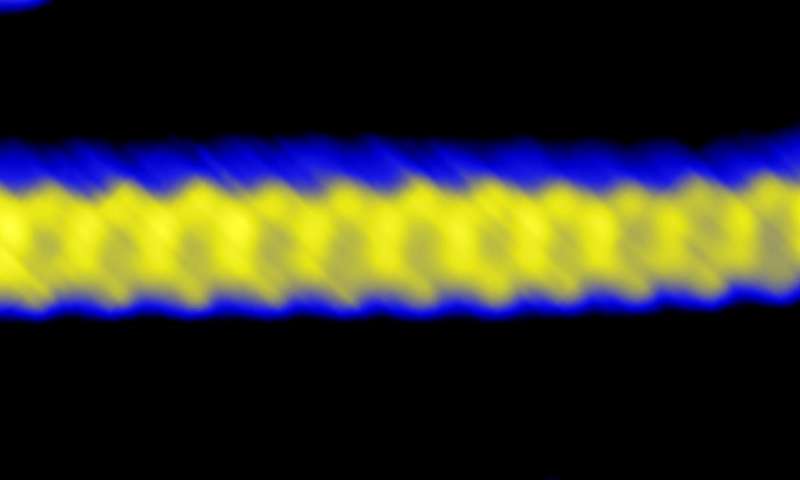
The team from ONRL, however, made semiconductive graphene with no other additional material by fashioning it in ribbons because when graphene becomes very narrow, it creates an energy gap. The narrower the ribbon is, the wider the energy gap and the ribbons made at ONRL are definitely narrow. One nanoribbon has a width of only one nanometer or less.
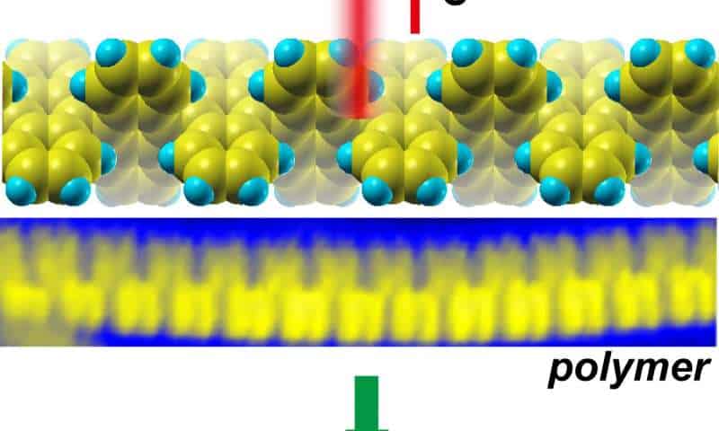
Besides narrowness, another important factor is the shape of the edge. When graphene’s hexagon is cut along the side, its shapes resembles an armchair — this shape enables the material to act like a semiconductor.
Previously, scientists made graphene nanoribbons by growing them on a metal substrate. This was necessary but undesirable because the metal hinders some of the ribbons’ useful electrical properties.

ONRL took a different route to get rid of the metal substrate altogether. To trigger chemical reactions that control the width and edge structure from polymer precursors, the team used the tip of a scanning tunneling microscope to inject positive charge carriers called ‘holes’. The reaction could be triggered at any point of the polymer chain by moving the tip in the right direction. This method rendered ribbons that were only seven carbon atoms wide whose edges were neatly wrapped in the armchair configuration.
“We figured out the fundamental mechanism, that is, how charge injection can lower the reaction barrier to promote this chemical reaction,” said An-Ping Li, a physicist at the Department of Energy’s Oak Ridge National Laboratory.
Moving forward, the researchers plan on making the heterojunctions with different precursor molecules. One exciting possibility is conducting photons in a new electronic device with graphene semiconductors where current could be carried with virtual no resistance even at room temperature — a life-long dream in solid state physics.
“It’s a way to tailor physical properties for energy applications,” Li said. “This is an excellent example of direct writing. You can direct the transformation process at the molecular or atomic level.”
Scientific reference: Chuanxu Ma et al, Controllable conversion of quasi-freestanding polymer chains to graphene nanoribbons, Nature Communications (2017). DOI: 10.1038/ncomms14815.


