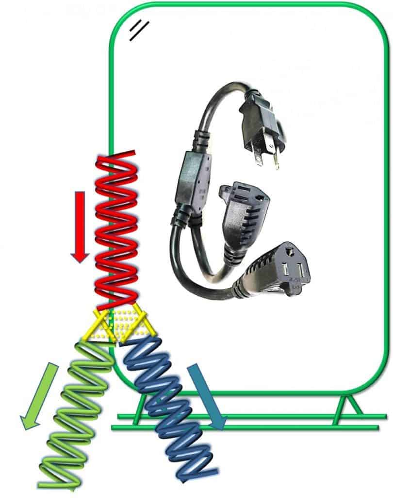
Besides carrying the genetic blueprint for all living organisms, DNA is also a versatile building block for practical affairs. Scientists are experimenting, for instance, with DNA as a storage device. One promising method can encode 215 petabytes of data — twice as much as Google and Facebook combined hold in their servers — on a single gram of DNA. Now, American researchers have found a way to use DNA in microelectronic circuits after they showed how to design, create, and use a DNA circuit capable of splitting and combining current. It works much like an adapter that can connect multiple appliances to a wall outlet.

DNA has remarkable self-assembly properties, which scientists previously exploited to great effect to assemble graphene transistors and to design new drugs. This works rather easily because the molecule’s four nucleotide bases (A, T, C, and G) can be programmed to self-assemble into the iconic double-helices, snapping together like matched puzzle pieces, A always bonding with T and C with G. Indeed, various 2-D and 3-D DNA structures have been synthetically designed by scientists in the past using this straightforward principle.
The double-helix molecule can also conduct electric charge over considerable distances. Combine this with self-assembly and you’ve got a very promising candidate for niche applications in electronics such as nanobots, photonic devices, or various tiny electronic circuits.
“The ability of DNA to transport electrical charge has been under investigation for some time,” said Nongjian “N.J.” Tao, a co-author of the new study researchers at Arizona State University. “Splitting and recombining current is a basic property of conventional electronic circuits. We’d like to mimic this ability in DNA, but until now, this has been quite challenging.”
There’s one problem though: In its most common duplex form, DNA poorly splits current into three or more terminals as the charge tends to dissipate at the splitting junctions or convergence points. This doesn’t bode well for electronics applications. However, scientists at Arizona State University, New York University, and Duke University, used a special form of DNA known as G-quadruplex (G4) DNA. As the name implies, G4-DNA is composed of four rather than two strands of DNA, which are rich in the nucleotide guanine (G).
“DNA is capable of conducting charge, but to be useful for nanoelectronics, it must be able to direct charge along more than one path by splitting or combining it. We have solved this problem by using the guanine quadruplex (G4) in which a charge can arrive on a duplex on one side of this unit and go out either of two duplexes on the other side” says Peng Zhang, an assistant research professor of chemistry at Duke University and a co-author of the new study.
“This is the first step needed to transport charge through a branching structure made exclusively of DNA. It is likely that further steps will result in successful DNA-based nanoelectronics that include transistor-like devices in self-assembling ‘pre-programmed’ materials,” Zhang says.
Guanine-rich quadruplex DNA occurs naturally, a configuration that can be found in telomeres — the ends of linear chromosomes, which play a key role in aging. Some research is targeting G4 quadruplexes with drugs for therapeutic reasons. Previously, research showed that DNA quadruplexes in telomeres decrease the activity of an enzyme responsible for telomere length and which is involved in 85 percent of all cancers.
Among other things, G4 DNA — stacked guanine bases that form hydrogen bonds with their immediate neighbors — have improved charge transport properties. This allowed the researchers to used G4 DNA and double-stranded wires to form the terminals for either splitting or merging electrical current flow. Previously, scientists who tried to make Y-shaped electrical junctions with conventional double-helix DNA failed because of the inherent poor charge transport properties.
The conductance of charge of the G4-DNA nanostructure was measured with a scanning tunneling microscope (STM), whose tip came in and out of contact with the molecule, breaking and reforming the junction while the current through each terminal is recorded. This “break junction” method allowed the researchers to fine-tune all sorts of prototype circuits to achieve maximal charge transport.
Besides opening the doors for innovative G4-based electronics, the paper published in Nature Nanotechnology sheds new light on the way nature maintains genetic integrity within cells, and could also teach us how various diseases break down DNA error-correcting mechanisms.


