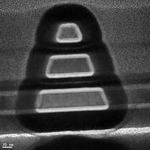
It’s amazing how this cross-section view on the right showcasing a new type of transistor from Purdue and Harvard universities resembles a Christmass tree, just in the nick of the time for the holiday season. Its design, however, has little to do with a Christmas trees. Make no mistake, the transistor’s shape and design follows a pattern that allows it to operate faster and possibly lead to a new generation of computers powered by it.
“It’s a preview of things to come in the semiconductor industry,” said Peide “Peter” Ye, a professor of electrical and computer engineering at Purdue University.
The transistor are made out of three nanowires progressively smaller, yielding a tapered cross section resembling a Christmas tree. Typically, transistors are flat, however the researchers’ design follows previous work where a 3-D structure was used. This allows for a significant improvement in performance by linking the transistors vertically in parallel.
“A one-story house can hold so many people, but more floors, more people, and it’s the same thing with transistors,” Ye said. “Stacking them results in more current and much faster operation for high-speed computing. This adds a whole new dimension, so I call them 4-D.”
Transistors are indispensable to electronic components since they regulate the flow of electricity, and thus information. These devices have what are called logic gates which either switch the transistor on and off and direct the flow of electrical current. The smaller the logic gate, the faster the operation time, and in turn performance.
In today’s high-end 3-D silicon transistors, the length of these gates is about 22 nanometers, or billionths of a meter. This is where silicon, however, has reached its limit and the future’s next generation transistors need to employ a different semiconductor in order to pass this threshold.
A new semiconductor shrinks transistors even further
Researchers from Purdue and Harvard universities created their transistor from a material that could replace silicon within a decade, called indium-gallium-arsenide. The material is among several promising semiconductors being studied to replace silicon. Such semiconductors are called III-V materials because they combine elements from the third and fifth groups of the periodic table.
And that’s not all either. In order to shrink transistor even further, another important design parameter, the insulating, or “dielectric” layer that allows the gate to switch off, also needs to be changed. Nanowires in the new transistors are coated with a different type of composite insulator, a 4-nanometer-thick layer of lanthanum aluminate with an ultrathin, half-nanometer layer of aluminum oxide.
Ultimately, the researchers transistors made of indium-gallium- arsenide with 20-nanometer gates, which is a milestone, Ye said.
Findings will be detailed in two papers to be presented during the International Electron Devices Meeting on Dec. 8-12 in San Francisco


