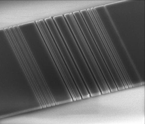
A breakthrough in optical communications has been reported by Stanford engineers who used a complex algorithm to design a prism-like device that splits light into different colours (frequencies) and at right angles. This is the absolute first step towards building a circuit, and ultimately a computer, that uses light instead of wires to relay signals. This way, much more compact and efficient machines could be built.
No metal wires

Professor Jelena Vuckovic and Alexander Piggott, a doctoral candidate in electrical engineering, initially developed an algorithm automated the process of designing optical structures and it enabled them to create previously unimaginable, nanoscale structures to control light. Now, for the first time, the team used this algorithm to build a pattern that resembles a bar code made up of alternating rows of silicon of varying thickness with air in between. The algorithm automatically built the design with the researchers only having to give the desired inputs and outputs they’d for the system.
The alternating rows are essential since this complex arrangement guides light in a predictable pattern based on the refraction indexes it encounters along the way. Light doesn’t actually travel at the speed of light, not here on Earth at least; the speed of light you and I leaned in school is measured in vacuum. In reality, light is effected by the medium through which it travels and as such, it’s speed and angle are altered. When light passes from air into water, you see a dislocated image. That’s because the light that bounced back into your retina, allowing you to see the object you immersed in the water, has passed into a medium with a higher index of refraction. Air has an index of refraction of nearly 1 and water of 1.3. Infrared light travels through silicon even more slowly: it has an index of refraction of 3.5.
Exploiting multiple refraction indexes from silicon and air, an ‘optical link’ was built that acts like a prism to split two different wavelengths (colors) at right angles to the input, forming a T shape. Both 1300-nanometer light and 1550-nanometer light, corresponding to C-band and O-band wavelengths widely used in fiber optic networks, were beamed at the device from above. When these hit the link, the lights were reflected opposite to each other.
Let computers do the hard work
The most beautiful part is that the algorithm did all the hard work.
“We wanted to be able to let the software design the structure of a particular size given only the desired inputs and outputs for the device,” Vuckovic said.
Of course, it took a lot of work and hundreds of tweaks from the researchers’ part to make it work in the first place. What’s great about working this, however, is that engineers can build any kind of patterns just by setting an input and output in the software. If they need different kinds of light or other geometries, they just leave it to the algorithm to calculate the optimal pattern. It all takes only 15 minutes to rend. Traditionally, optical manipulation was made a on a case by case basis requiring a lot of trial and error. This saves hundreds of hours of hard work.
“For many years, nanophotonics researchers made structures using simple geometries and regular shapes,” Vuckovic said. “The structures you see produced by this algorithm are nothing like what anyone has done before.”
Besides the optical link, the team used the algorithm to design other devices as well, such as the super-compact “Swiss cheese” structures that route light beams to different outputs not based on their color, but based on their mode. These were used to split light modes, which is essential to optical communications for transmitting information.
Findings appeared in Scientific Reports.


