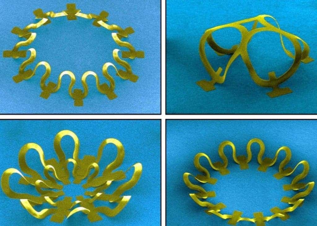
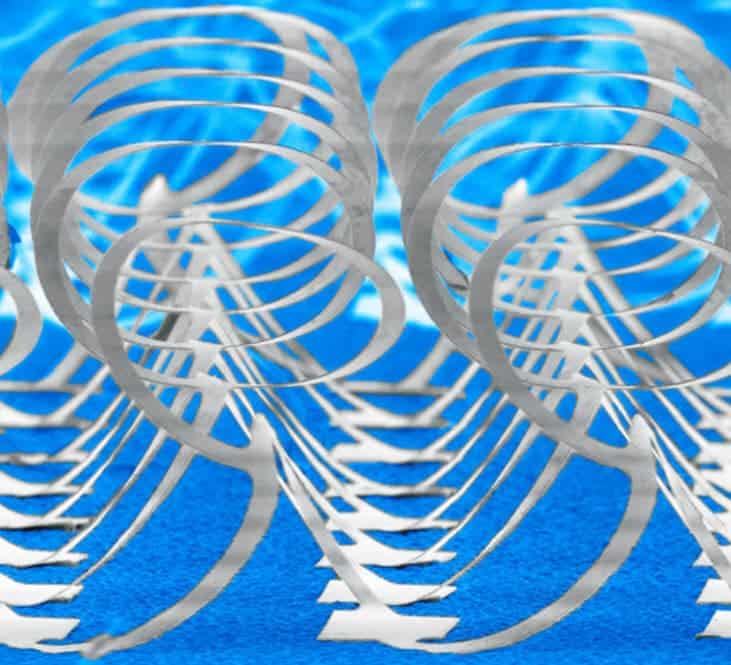
Everybody’s excited about 3-D printing, but let’s put it aside for just one second. Researchers at Northwestern University and the University of Illinois at Urbana-Champaign recently demonstrated a new technique for building complex and very fine 3D micro and nano structures out of 2-D shapes. The whole process is very similar to how a children’s pop-up book works, starting as a flat 2D surface only to expand into a 3D shape when prompted. The authors note that the pop-up method has various advantages over 3D printing, including use of multiple materials during the fabrication process and integration with electronics.

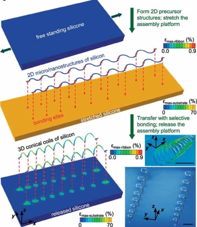
“In just one shot you get your structure,” said Northwestern’s Yonggang Huang, one of three co-corresponding authors on the study. “We first fabricate a two-dimensional structure on a stretched elastic material. Then we release the tension, and up pops a 3-D structure. The 2-D structure must have some place to go, so it pops up.”

Basically, the method exploits compression buckling, combining strong points of adhesion with weak points between the 2D structure placed on an elastomer. When the tension from the stretch is released, the compression buckling takes over. The strong adhesion points stay in place, while the weak ones break away. In the end, a 3D predictable structure pops out.
“A key, unique feature of these approaches to 3-D microarchitectures is that they work equally well with a very wide variety of materials, including the highest performance semiconductors, such as device-grade silicon, and fully formed, state-of-the-art planar devices and systems,” said John A. Rogers, the paper’s third co-corresponding author and a Swanlund Chair and professor of materials science and engineering at the University of Illinois. “We believe, as a result, that these ideas have relevance to nearly every class of microsystem technology — from electronics to photonics, optoelectronics, microelectromechanical structures and others.”

The pop-up method is exciting because it’s fast and inexpensive, with the added advantage over 3D printing of being capable of integrating more than one material in the structure. It’s also possible to build semiconductors or single crystalline metals, two important requirements in modern manufacturing today very difficult to achieve if not impossible using 3-D printing. Using this novel technique, scientists can build structure on both micro and nano scales down the thickness of only 100 nanometers. The resulting geometries, made using computer models, can be of intricate complexity.
Scientists at Zhejiang University, Hangzhou, China; Hanyang University, Seoul, Korea; and East China University of Science and Technology, Shanghai were also involved in the study. The U.S. Department of Energy supported the research. The paper appeared in the journal Science.


