Counting microscopic particles is hard, but researchers from Russia and Australia believe they’ve found a way to make it easier.

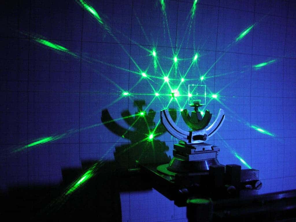
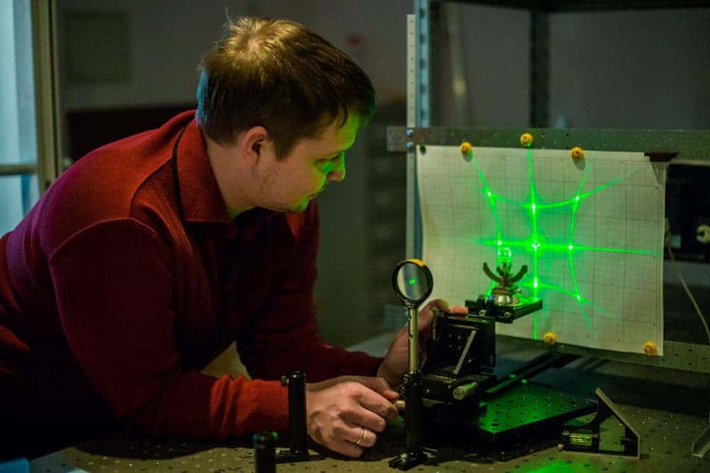
The principle is fairly simple. A research team from ITMO University, Ioffe Institute, and Australian National University passed a laser beam through an optic material riddled with microscopic particles and then projected it onto a screen. The screen showed a characteristic pattern consisting of numerous bright spots and the number of these bright spots corresponded to exactly to the number of scattering microscopic particles in the optical material.
“The light senses heterogeneity,” says Mikhail Rybin, first author of the paper, senior researcher at the Department of Nanophotonics and Metamaterials at ITMO University.
“We found out that by looking at the pattern it is possible to determine the precise number of scatterers in the material. This helps understand not only the type of the sample lattice (square, triangular), but also establish its structure (20 to 20 particles, or 30 to 15) just by counting the light spots on the screen”.
It’s very simple but also very effective. You shine a laser beam through the material and then onto a projector. The different structure of the material will cause light to diffract, and the result will be visible on the projector.
“Depending on the shape and relative position of the scatterers, the light wave continues to propagate differently behind the sample. In other words, the structure of the sample affects the diffraction pattern, which will be projected on the screen.

The new method is a much more affordable option to expensive electron or atomic force microscopy and doesn’t damage the sample at all. It’s also extremely easy to use.
“Even a schoolboy can buy a laser pointer, adapt a small lens to focus the light better, fix the sample and shine a laser beam on it,” notes Mikhail Rybin. “In addition, our method makes it possible to study optical materials without changing their structure, in contrast to electron microscopy, where the sample surface has to be covered with conductive metal layer, which impairs optical properties of the sample”.
The method can be extremely useful for constructing and assessing metamaterials. They tested it for two classes of such materials: photonic crystals and metasurfaces. Photonic crystals are periodic optical nanostructures which affect the motion of photons in much the same way that ionic lattices affect electrons in solids. When light passes through one, it generates a fancy pattern on the screen behind the sample.
In the case of a metasurface – an artificial sheet material – things are a bit more complicated because the material has to be constructed in such a way that the distance between particles is significantly smaller than the wavelength of light. In fact, the difference between a photonic crystal and a metasurface depends on the wavelength of the light.
“For one wavelength, the material will act as a photonic crystal and as a metasurface for another. That is why designing such structures, we can evaluate maximum lattice period with laser,” concludes Mikhail Rybin.


