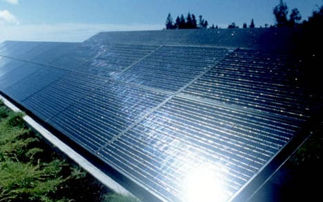
Researchers at the University of Illinois at Urbana-Champaign report they’ve devised a new type of highly efficient solar cell that is potentially easier to manufacture and cheaper than cells of similar performance. The stacked cell allows photon energy to be garnered from across the whole solar spectrum, and this new design makes use of a novel technique which basically electrically insulates each stack of the cell from each other – something previously deemed unpractical.
One, two, three, four cells
Most commercial solar cells today, the amorphous or noncrystalline silicone cells you see hung over most rooftops, have a top rated efficiency of around 20%. These are single-junction cells that have performance constraints defined by their Shockley–Queisser limits. A single junction means that the cell is comprised of only one type of photon absorbing material or only one bandgap. If the energy of a photon is lower than that bandgap, the photons will simply pass through the material, while higher bandgap photons will release their energy as heat, thus becoming wasted.
Multi-junction cells, however, employ a nifty trick to squeeze as much energy from photons as possible. By layering multi bandgap materials one over the other, you can transform more of the incoming energy into displaced electrons, hence more electrical power and considerably improve efficiency. This way high energy photons are captured in a large bandgap layer on top, while lower energy photons that pass through are captured in a small bandgap layer underneath, can push efficiency above 40%. Solar companies with efficient solutions for solar projects commonly employ these sort of cells.
The idea sounds extremely simple and some might wonder how come engineers didn’t thought of this sooner. They have, trust me, since the early ’60s when solar power was an emerging technology with a lot of attention focused on it. The truth is, multiple junction cells are extremely difficult to design. Different currents are generated in the different layers, charge builds up at the edges of layers, opposing the applied electric field and lowering the cell’s efficiency. Therefore, the layers have to be carefully designed so that the currents match.
‘People have worked out how to manage this in two or three junctions,’ explains author John Rogers of the University of Illinois at Urbana-Champaign. ‘When you get to four, five or six, it becomes more and more daunting.’
A new world record
What you can do, alternatively, is to keep each layer electrically insulated from the other and individually collect electrons, but so far there’s no reliable industrial process for scaling such a sort of cell. This may change in the future.
Rogers and his team started with a three-layer design that, until recently, held the world efficiency record at about 42%. They chopped up a germanium wafer into tiny pieces and mounted the individual cells in a printed circuit board arrangement. They covered the germanium wafers with a very thin layer of electrically insulating arsenic triselenide glass and used lithography techniques to print tiny versions of the three-layer cells on top. Just by placing two small electrodes between the cells, electrons were collected from the two cells separately.
‘This is a first demonstration out of the box,’ Rogers explains. ‘It’s not a one-shot demo.’
While the efficiency of their quadruple-junction cell was only improved by 1.8% (43.9% at concentrations exceeding 1,000 suns), the researchers conclude that ‘this technology is the lowest cost solution for climates that offer high levels of direct sunlight, such as solar cells deployed in arid environments […] The cost of energy is projected to be lower than that of coal-fired power plants.’
Since the materials and manufacturing techniques are compatible with large-scale manufacturing, indeed this projects seems very feasible.
The inventors of the multijunction solar cells were also recently award a $1 million prize


