Moore’s law says that the number of transistors in an integrated circuit doubles every two years, hence doubling also the computing power. Since it was first predicted in 1965, this trend has hold true allowing computers to evolve at an exponential rate. To support the law, scientists tweak one or all of these three main manufacturing parameters: chip size, speed and price. Now, a new dimension might be factored in: tallness.
Making chips in 3-D
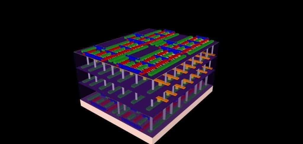
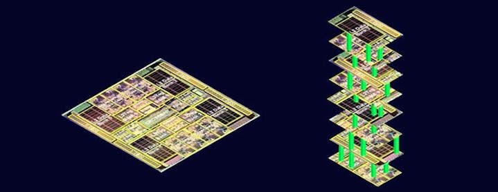
Researchers at Stanford University show how this might happen after they revealed a novel manufacturing technique which can be used to make multi-story logic and memory chips. Of course, scaling chips vertically has been considered before but it wasn’t until recently that the numerous challenges that come with it were overcome. The main issues are operating temperature (lost electrons transform into heat and the more circuits you have packed the more heat generated) and so-called traffic jams that happen when computers get too busy.

The approach ingeniously stacks both logic and memory chips atop one another, interconnecting them with thousands of nanoscale electronic “elevators” that move data fast between the layers. This would allow data to flow faster and using less electricity, than the traditional bottle-neck prone wires connecting single-story logic and memory chips today.
“This research is at an early stage, but our design and fabrication techniques are scalable,” said Subhasish Mitra, a Stanford professor of electrical engineering and computer science. “With further development this architecture could lead to computing performance that is much, much greater than anything available today.”
The de facto material used for making transistors and computer chips today is silicon. The material has proven to be a great fit for the electronics industry, but it’s now nearing the full extent of its capabilities. One problem with silicon is heat. We all feel this when we hold a smartphone and put our hands over a computer. This heat is in fact electricity that leaks out of the silicon transistors. To solve this problem, Stanford researchers turned to carbon nanotubes
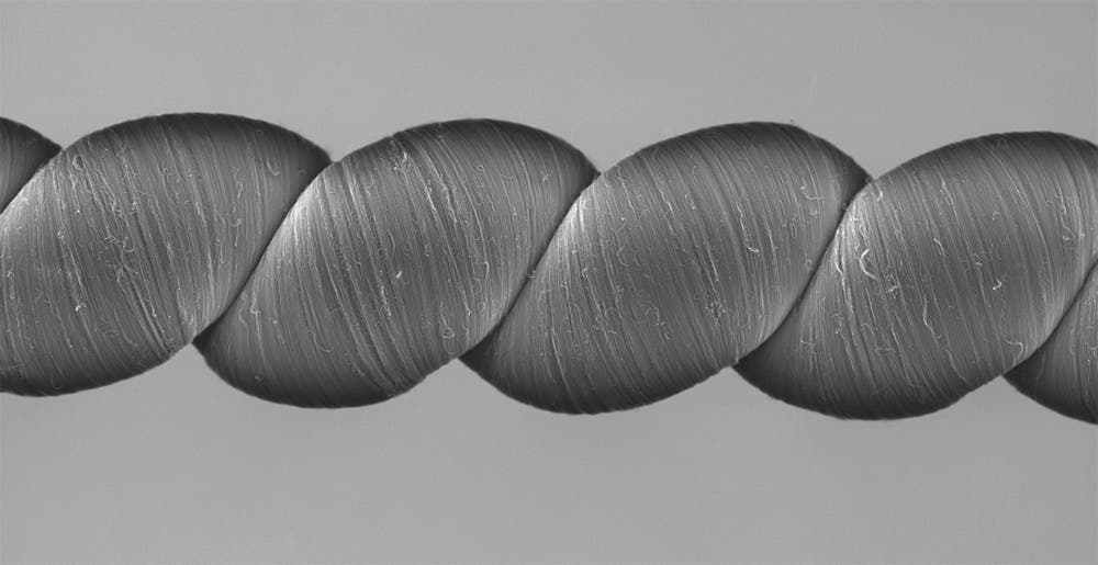
Carbon Nanotubes (CNTs) and their compounds exhibit extraordinary electrical properties for organic materials, and have a huge potential in electrical and electronic applications such as photovoltaics, sensors, semiconductor devices, displays, conductors, smart textiles and energy conversion devices (e.g., fuel cells, harvesters and batteries). They are so slender that nearly 2 billion CNTs could fit within a human hair. Because of their tiny diameter, CNTs are thought to lose less electrons, but packaging enough of them to became effective has proven to be difficult.
Mitra and colleagues employed a nifty trick. They started by growing CNTs the standard way, on round quartz wafers, then added a metal film that acts like a tape. Just like an adhesive, when a silicon wafer was placed atop, the CNTs came off the quartz growth medium. To make sure they made a CNT layer with sufficient density the lift and deposit technique was repeated 13 times. The researchers report they achieved some of the highest density, highest performance CNTs ever made – an impressive feat considering they didn’t have sophisticated equipment at their disposal like those at a commercial plant.
The CNTs were only one part of the equation – the logic part for the transistors. They still had to figure out how to make memory for vertical chips. So, again they devised a storage medium that isn’t based on silicon, like most of today’s RAM. Instead, the Stanford team fabricated memory using titanium nitride, hafnium oxide and platinum. This formed a metal/oxide/metal sandwich. Applying electricity to this three-metal sandwich one way causes it to resist the flow of electricity. Reversing the electric jolt causes the structure to conduct electricity again. Changing from resistance to flow is how this new memory type creates digital zeroes and ones, hence the name resistive random access memory, or RRAM.
Authors write that RRAM uses less energy, which translates into a prolonged battery life for smartphones or notebooks.

Ultimately, Max Shulaker and Tony Wu, Stanford graduate students in electrical engineering, unveiled a four-story high-rise chip at the IEEE International Electron Devices Meeting in San Francisco. There, they explained the key parameter that helped them achieve this amazing feat: manufacturing temperature. Typically, memory or transistors from silicon are manufactured at very high temperatures of around 1,000 degrees Celsius. The Stanford process for making RRAM and CNTs uses low temperature so they could stack memory and logic boards atop one another without risking melting anything below.
Now, imagine not four but eight, sixten or 512 of these layers stacked. You’d get a chip that’s 512 times more powerful than the same ones found today that occupy the same surface area. Truly, this has the potential to change computing. Before you make your hopes up for a quantum computer of your own at home (better wait until someone actually makes one in the lab first), you might want to consider paying more attention to this sort of advances.


