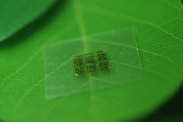
Researchers at the University of Wisconsin-Madison designed an innovate and sustainable solution to the global electronic waste problem: make the substrate of computer chips out of cellulose nanofibril (CNF), a biodegradable material from wood. The team collaborated with the the Madison-based U.S. Department of Agriculture Forest Products Laboratory (FPL) to build their device.

A cellulose nanofibril (CNF) computer chip rests on a leaf. Photo: Yei Hwan Jung, Wisconsin Nano Engineering Device Laboratory
On average, cell phones are used for less than 18 months and computers are used for some 3 years before being replaced. But very few end up getting recycled, in part because there’s little awareness on the subject, part lack of facilities. Not to mention how prohibitively expensive it can be to extract the toxic semiconductors that makeup the devices, like gallium arsenide (GaAs). So, most electronics end up in the landfill, polluting the environment and expanding demand for further landfill space.
Wood is plentiful and biodegradable, so why not chop some good ol’ chips? Trust me, I was as skeptical as you at this point until I read the paper (Nature). According to the researchers at UW, the active region of a typical computer chip is only a thin layer atop a bulk support which consists of more than 99% of the semiconductor material. This huge bottom layer relative to the top layer is basically used only to carry non-active components. As such, it can be replaced with just about any material, in this case a favorable biodegradable one, granted chip operation isn’t affected.
“The majority of material in a chip is support. We only use less than a couple of micrometers for everything else,” says UW-Madison electrical and computer engineering professor Zhenqiang “Jack” Ma. “Now the chips are so safe you can put them in the forest and fungus will degrade it. They become as safe as fertilizer.”
How about that – electronic fertilizer. You definitely don’t hear that every day. Naturally though the researchers didn’t build a chip atop of a wooden plank. First, the researchers had to breach two key barriers when dealing with wood-derived materials in an electronics setting: surface smoothness and thermal expansion. In the end, they found an elegant solution by coating the CNF layers with a special solution.
“You don’t want it to expand or shrink too much. Wood is a natural hydroscopic material and could attract moisture from the air and expand,” Zhiyong Cai, project leader for an engineering composite science research group at FPL. “With an epoxy coating on the surface of the CNF, we solved both the surface smoothness and the moisture barrier.”
With over a decade of experience working with CNF, the researchers are confident in their design. They say it can also be easily adapted to current manufacturing technology.
“The advantage of CNF over other polymers is that it’s a bio-based material and most other polymers are petroleum-based polymers. Bio-based materials are sustainable, bio-compatible and biodegradable,” Gong says. “And, compared to other polymers, CNF actually has a relatively low thermal expansion coefficient.”
Yei Hwan Jung, a graduate student in electrical and computer engineering and a co-author of the paper, says the new process greatly reduces the use of such expensive and potentially toxic material.
“I’ve made 1,500 gallium arsenide transistors in a 5-by-6 millimeter chip. Typically for a microwave chip that size, there are only eight to 40 transistors. The rest of the area is just wasted,” he says. “We take our design and put it on CNF using deterministic assembly technique, then we can put it wherever we want and make a completely functional circuit with performance comparable to existing chips.”


