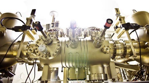
Dubbed MBE, after the intricate molecular beam epitaxy process, this device developed by scientists at Sharp Laboratories in Oxford, England, can actually grow electrical components at a dazzling precision atom by atom.
This is where razor sharp technology is at, as far as manufacturing goes, and this monstrous-looking device is capable of transferring atoms from one place to another almost individually, as tiny crystalline structures are layered together to form objects and thus build the basis of high tech electronics.
Using the MBE, Sharp engineers were able to build anything from lasers to LEDs and even solar panels. It’s a highly complex and demanding machine, however, one which requires almost space like vacuum inside of the working chamber for components to come out like they’re supposed to. Without vacuum, impurities would make the properties of the layered molecules useless and disrupt the whole process.

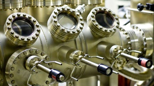
Inside of it, although perfectly isolated from the rest of the world and trapping a little piece of cosmos into its belly, the whole MBE process is fully controlled by the scientists who can dispose molecules in any they see fit. The whole operation is maneuvered through use of magnetic poles, with a handle on the outside of the MBE, to move the wafer into position. A pyrometer lets operators measure temperature remotely too, and despite being separated by a physical barrier, it’s possible for the scientists to have complete control.
RELATED: Smallest 3D printer
Dr Ian Thompson, Director of Business Development at Sharp Laboratories of Europe explains that “whatever your substrate is, the crystal structure will be what the first atom mimics. Whatever you layer on top follows its orientation.” The process is very controlled and, inside the MBE, a component literally grows before scientists’ eyes through the tiny circular viewing windows along its edge.
An interesting profile of the MBE machine can viewed below directly from one of Sharp’s leading engineers.
source: Human Invent


