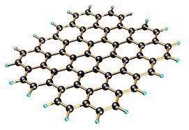
It seems scientists have yet to draw the line on where graphene, man’s greatest material ever discovered, ceases to amazes with its new abilities, since apparently new properties and uses for the carbon allotrope are found constantly. Most of the contributions come from University of Manchester, where the material has been recognized for its true history-shaping potential and where a state-of-the-art National Graphene Institute is currently being built. The latest discovery, indeed, hails from the same Manchester University where scientists were baffled themselves to find that graphene, a 2D structured material, can be used as basic building block for creating 3D crystal structures which are not confined by what nature can produce. The potential impact this could have on the electronics industry development is significant, by increasing efficiency.
This method may well open up a new aspect of physics research. The research shows that a new side-view imaging technique is able to be used to visualize the individual atomic layers of graphene inside the devices they have built. They discovered that the structures were nearly perfect, even when in excess of 10 different layers were used to build the stack, resulting in multilayer heterostructures and devices with designed electronic properties.
The side view imaging approach works by extracting a thin slice from the centre of the device. The researchers used a beam of ions to cut into the surface of the graphene and dig a trench on either side of the section they wanted to isolate.
The difference is that our slices are only around 100 atoms thick and this allows us to visualise the individual atomic layers of graphene in projection,” commented Dr Sarah Haigh at the University of Manchester’s school of materials. “We have found that the observed roughness of the graphene is correlated with their conductivity.”
This result indicates that the latest techniques of isolating graphene could be a big step forward for engineering at the atomic level as well as giving more weight to graphene’s suitability for next gen computer chips.
The scientists’ results suggest a leap forward for atomic-level engineering, and add more weight to the possibilitiy of seeing graphene as a sustainable solution for next-generation’s computer chips. Here’s how I described in short graphene’s properties a while back, when we found out that graphene can actually repair its structure automatically simply by substituting carbon atoms from its environment.
“It’s so thin, it can be molded into sheets just 1 atom thick, yet despite this, it’s so strong that you can actually pick it up. It has the highest current density (a million times that of copper) at room temperature, the highest intrinsic mobility (100 times more than in silicon), and conducts electricity in the limit of no electrons. Also, graphene now holds the record for conducting heat — it’s better than any other known material. But wait, there’s more – graphene is the most impermeable material ever discovered – so neatly packed together, that not even helium atoms can squeeze through.”
Yes, we’re pretty excited about graphene. If you understand what graphene can do for technology and human kind in the following decades, you’d be as well. Demonstrating graphene’s remarkable properties won Professor Andre Geim and Professor Kostya Novoselov the Nobel prize for Physics in 2010.
Professor Novoselov said: “Although the exciting physics which we have found in this particular experiment may have an immediate implementation in practical electronic devices, the further understanding of the electronic properties of this material will bring us a step closer to the development of graphene electronics.”
Professor Geim added: “The progress have been possible due to quantum leap in improvement of the sample quality which could be produced at The University of Manchester.”
Findings were published in the journal Nature.


