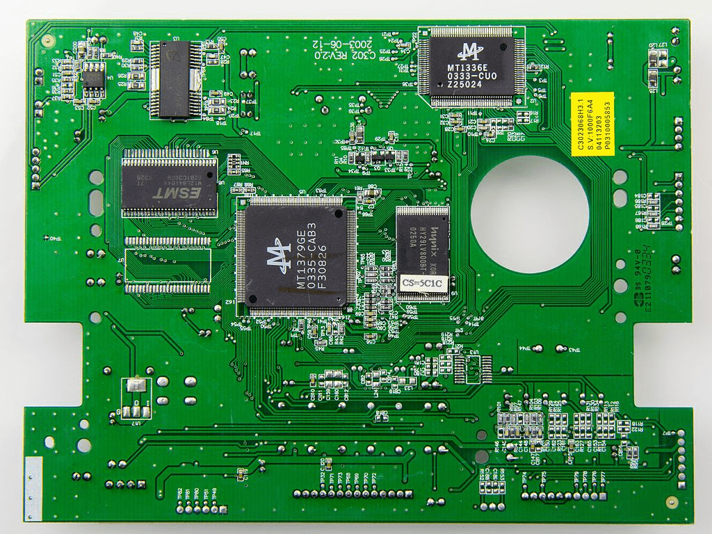
These days, almost everything has circuits and chips in it — and printed circuit boards (PCBs) are at the heart of circuits. We create and use an ungodly amount of PCBs, and more often than not, these are not recycled or reused. To make matters even worse, PCBs contain various pollutants that can harm the environment.
This is why having an alternative to print circuits on (especially an eco-friendly alternative) is so appealing. But using something biological came as an unexpected solution. In fact, researchers found that they can use mushroom skins for printing circuits on almost by mistake.

The age of myceliotronics
PCBs or circuit boards have various chemical components that are hard to separate and recycle. But mushroom skin degrades easily in the presence of light.
Many mushrooms have a protective skin that is thin but can be quite rough. Martin Kaltenbrunner, a soft matter physicist and professor at Johannes Kepler University in Austria, wanted to see if they can be used in electronics. He particularly looked at a mushroom called Ganoderma lucidum, a type of mushroom that grows on decaying hardwood trees. The dried skin of this mushroom is known to be thin and flexible, but also capable of retaining its structural integrity. Whatsmore, the mushroom is capable of withstanding temperatures of over 200 degrees Celsius (390 degrees Fahrenheit), which is essential for a material on which electronic circuits will operate.

Kaltenbrunner has been looking at fungi for some time, but not for electronics. He was looking more toward ways to use mycelium materials as an alternative to styrofoam. However, when they realized that the mushroom skin has all the desired properties for using as a base for circuits, they immediately realized its potential. In fact, the mushroom skin is even flexible, and doesn’t need to receive any special treatment: if you dry it, it can already be used to print circuits on.
However, mushrooms don’t conduct electricity. In order to bypass that, the researchers layered copper and chromium on top of it (and gold, in some cases). They then used lasers to create the circuit pattern onto the metalized mushroom skins. The result was almost as conductive as a standard PCB, but fully biodegradable and recyclable — the researchers found they can remove and reuse these printed layers easily using a heat gun or solder iron.

They call the material MycelioTronics, a play on words from “mycelium” and “electronics”. If kept out of UV light, the material can last for hundreds of years and serve as an efficient alternative to conventional, polluting PCBs.
However, this was only tested in a lab, not with real-world devices. The results are encouraging, but before we can usher in an age of myceliotronics, we need to be certain they work well in real-world scenarios, and this is exactly what researchers want to try out next. Still, at the very least, the dried mushroom skins can be used in things like casings or battery separators, the researchers say.
But if it does work, it could help the electronics industry lower its environmental footprint. Around 50 million tons of e-waste is generated every year, and the figure keeps growing — that’s more than the weight of all commercial airplanes ever produced. While not all of that is PCBs, of course, it’s an important part of it. Meanwhile, the mushroom-based material can not only be recycled, but also grown sustainably from only waste wood.
The study was published in Science Advances.


