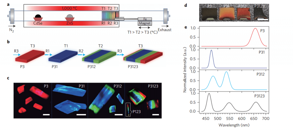
In what can only be heralded as a major breakthrough, a group at Arizona State University reports the demonstration of the first ever white laser – a laser that emits light over the full spectrum of visible colors. Up until now, lasers were designed to emit a distinct spectrum, either red, green, blue and so on. Combining multiple colors has always proved challenging and previous attempts had been slumped with shortcoming. This latest version seems to work wonderfully. If this technology can and will be scaled commercially, it could radically transform the industry. Its contrast and lighting capabilities, watt per watt, are well over LEDs and, moreover, it could help devise a new generation of Wi-Fi, called Li-Fi, which works on laser light and is 10 times faster.
The main problem that engineers encounter when building a full spectrum laser light is placing the mismatching crystals responsible for each color. When excited, each crystal gives off a certain light. Combine various crystals and you eventually end up with a white light laser, or so the theory goes. But that’s definitely easier said than done. Fortunately, the team led by Cun-Zheng Ning, a physicist and electrical engineer at Arizona State University at Tempe, found the right combination.

the region used for positioning the substrate (see Supplementary Section 5 for more details). b, Illustration of the growth procedure. Samples are grown
starting at position R3, then at positions R1, R2 and finally back to R3, with corresponding temperatures labelled T1, T2 and T3. The associated product
samples after these steps are labelled P3, P31, P312 and P3123, respectively, where the numbers following ‘P’ represent the growth sequence at various
locations. For example, P312 represents a product grown first at R3, followed by growths at R1 and then at R2. c, Photoluminescence images of individual
structures after the corresponding growth sequences. Note that the images were taken after the structures were transferred onto a glass substrate from their
as-grown ones using a contact printing method. Inset in rightmost panel a multi-segment nanowire structure resulting from the P123 growth sequence. Scale
bars, 15 μm. d, Optical images of the samples under ambient lighting. Scale bar, 1 cm. e, Photoluminescence spectra of the samples shown in c,d. Image: Nature
The center piece of their design is an extremely thin sheet made from a semiconductor alloy. The sheet is divided into multiple segments, each being a different alloy of zinc, cadmium, sulfur, and selenium. When the cadmium and selenium-rich segments get excited, this give off a red light, cadmium and sulfur-rich segments give off green light, while zinc and sulfur ones glow in blue. By carefully controlling the vapor, liquid, and solid phases of each crystal, the researchers were able to make the crystals interplay and join together to give off an overall full spectrum white light.
By varying the power each segment received, the researchers could tweak the intensity. In doing so, they came up with 70 percent more perceptible colors than the most commonly used light sources. They’re also very energy efficient. You can a lot with an LED light, which gives off 150 lumens per watt of electricity. For a fraction of the power of a halogen bulb, you can light up a room with LEDs. With white lasers you can go even further since these give off 400 lumens per watt of electricity. Ten years from now, the video displays of the future might all be based on white lasers, offering more colors and a higher contrast than ever.
Additionally, one could use the white lasers as Wi-Fi. Wi-Fi based on light is called Li-Fi, and there are already current efforts that experiment with LEDs. These are reportedly 10 times faster than Wi-Fi. Who knows what kind of signal transfer you can get with white light lasers. This has definitely been a good day for science.
Findings appeared in Nature.


